

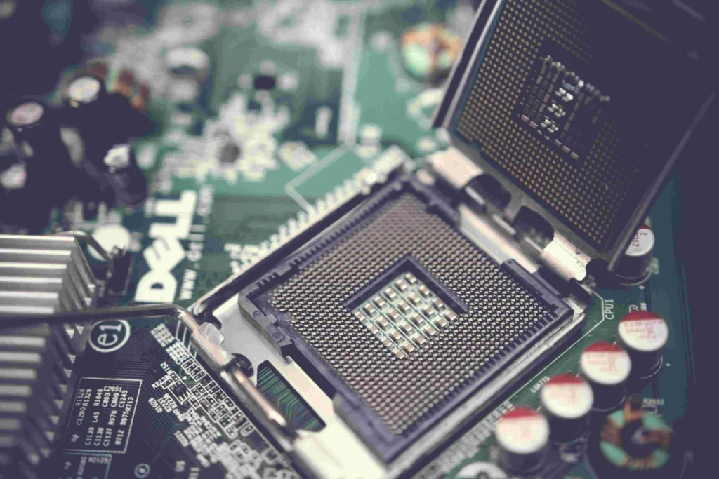

The global race to build out artificial intelligence infrastructure has triggered multi-billion-dollar investments in advanced chip packaging. Once viewed as a mundane final step in manufacturing, packaging has evolved into a critical bottleneck in producing the world’s most powerful processors. With demand for AI chips heavily outstripping existing capacity, industry leaders like Nvidia and AMD, alongside specialized Taiwanese subcontractors and equipment makers, are aggressively expanding production lines and developing new tooling. Speaking recently in Taipei, former Intel CEO and current Playground Global partner Pat Gelsinger noted that packaging was historically an afterthought, yet it could soon represent up to half the total value of a semiconductor product, as modern GPUs and CPUs increasingly integrate 10 to 20 individual chiplets. According to research firm Yole Group, revenues from advanced packaging are projected to surpass traditional packaging for the first time in 2026, with capital expenditures in the sector approaching $28 billion.
A Architectural Shift and TSMC’s Dominance
This investment surge reflects a fundamental transformation in chipmaking. For decades, packaging merely protected silicon dies and connected them to circuit boards. Now, as shrinking transistors becomes prohibitively expensive and physically challenging, engineers use advanced packaging to fuse multiple components—such as logic processors and high-bandwidth memory—into a single unified system. This architecture dramatically accelerates massive data transfers, a vital requirement for training and operating AI models.
Taiwan’s TSMC currently dominates this sphere through its proprietary chip-on-wafer-on-substrate (CoWoS) technology, serving heavyweights like Nvidia, AMD, Broadcom, and major cloud providers. However, severe capacity constraints at TSMC are forcing chip designers to secure alternative supply chains. According to industry sources, Nvidia is channeling billions of dollars into Siliconware Precision Industries (SPIL), a subsidiary of Taiwan’s ASE Technology, to fund factory expansions and tooling for CoWoS production. Similarly, AMD has committed over $10 billion across Taiwan’s semiconductor ecosystem, partnering with ASE, SPIL, and Powertech. While AMD CEO Lisa Su reaffirmed TSMC’s status as an indispensable partner, she emphasized that the industry urgently requires broader overall capacity for high-performance computing.
The Push for Alternatives and Equipment Innovation
TSMC’s tight supply has created a lucrative opening for smaller players like Taiwan’s Powertech Technology (PTI), whose chairman, D.K. Tsai, pointed out that tech companies are actively seeking ways to avoid single-source reliance on TSMC. PTI is heavily backing panel-level packaging, which replaces traditional round silicon wafers with larger rectangular panels. This format accommodates more chips per batch and minimizes material waste—an advantage for oversized AI processors that Microsoft Azure hardware chief Rani Borkar also highlighted. PTI is already collaborating with AMD and Broadcom on the technology and plans to invest $400 million in a Singapore-based joint venture with Broadcom, targeting production by 2028. Meanwhile, TSMC is countering with its own panel-based solution, chip-on-panel-on-substrate (CoPoS), having established a pilot line in April with commercial rollout expected within a few years.
This packaging boom is simultaneously reshaping the semiconductor equipment sector, which traditionally focused on front-end silicon fabrication. Executives at Tokyo Electron Taiwan and U.S.-based Applied Materials note that demand for advanced packaging machinery is expanding far faster than conventional chipmaking gear, projecting that the market—including panel-level formats—will scale dramatically over the next three to five years.